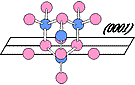
DID has reported extensively on research contracts related to Gallium Nitride (GaN) semiconductors, which offer significantly higher power and performance. Unfortunately, they present manufacturing and cost challenges that have stymied their use in commercial applications.
In May 2005, Compound Semiconductor Magazine offered an excellent overview of the GaN wide-bandgap semiconductors program and DARPA’s goals. Key program objectives include rapid transition of the technology developed into military systems. Other important goals include a “great” improvement in understanding the physical reasons behind device failures and the development of physical models to predict performance, reproducible device and MMIC fabrication processes, and improved thermal management and packaging. Reliability is expected to be a key challenge.
GaN represents an innovation in materials technology. DARPA’s approach adds innovative procurement strategies, via a 3-pronged approach that aims to speed the development of GaN-based microelectronics…
DARPA’s GaN Tracks
While DARPA’s development of GaN has been small in comparison to the Gallium Arsenide MIMIC program of the early 1990s, they’re trying to fast-track GaN development by removing the intermediate step between the technology-development programs and system insertion. In the second phase of the current efforts (denoted “Phase III”), project partners will be under instructions to come up with business plans that will identify system-insertion points at the earliest opportunity.
By taking this relatively aggressive approach, some believe that the commercialization process can be moved forward by 3-5 years. If all goes well, module development and engineering may commence in around 5-6 years, while volume production could become a reality within a decade.
Track 1 relates to an X-band transmit/receive module containing both power-amplifier and low-noise amplifier MMICs. Raytheon is the lead contractor on an initial $26.9 million contract, which features an alliance with Cree and options that could expand it to $59.4 million.
Track 2 is focused on a Q-band high-power amplifier module; it is headed up by Northrop Grumman Space Technologies (NGST) and could eventually be worth up to $53.4 million. For NGST, the focus is on moving its GaN research and development work into volume production – the demand from DARPA is for at least 384 three-inch wafers to be delivered over the course of the program. NGST’s ultimate goal is to produce a Q-band (> 40 GHz) module with a continuous-wave power output of 20 W.
Historically, NGST worked on the MIMIC Gallium Arsenide (GaAs) development program in the early 1990s, and also on the successful development of InP-based MMICs that are used today in advanced satellite applications.
Track 3 requires the development of a 2-20 GHz high-power amplifier module. TriQuint worked with BAE, Nironex, and academic partners to take charge of Track 3 in February 2005, via a contract worth an initial $15.8 million, plus options up to $31.7 million.
Track 3 aims to produce a wideband high-power amplifier module operating at frequencies of 2-20 GHz for applications such as jamming and electronic attack, but the improved X-band output, efficiency, and higher frequencies/higher gain will have civilian spin-offs as well in satellite links, cellular backhaul, et. al. For TriQuint, the 18 month technological goals (table 2) call for a wideband device operating at 40 V with 39 dBm continuous-wave output power, 12 dB gain and a power-added efficiency (PAE) of 60%. TriQuint’s state-of-the-art performance is exhibited by a 40 V, 1 mm device with an output of 5 W/mm at 10 GHz, 11-12 dB gain and a PAE of a little under 50%. BAE Systems has vast experience in making GaN-based low-noise amplifiers on native GaN substrates, but the manufacturing process will be finalized at TriQuint.
In all three tracks Silicon Carbide (SiC) will be the substrate material of choice. A crucial part of the project’s initial 2 years (Phase II) will involve gaining a more thorough understanding of the effects of different substrate types on device performance.
Additional Contracts and Key Events

June 2/09: TriQuint Semiconductor received a $15.8 million contract for Phase III of a multi-year gallium nitride (GaN) research and development contract from the Army Research Laboratory (ARL) in Adelphi, MD. This is DAPRA’s Track 3, above, and the project is funded by DARPA.
TriQuint began execution of the previous Phase II contract in 2005, and this award brings them to the contract’s expected maximum of $31.7 million. The Phase III contract (W911QX-05-C-0087) is focused on extending device reliability for 48V operation, while increasing operational lifetime and performance to cover the high end of contracted frequency ranges. For the Phase III contract, TriQuint is still teamed with BAE Systems, and adds IQE-RF Corp., and Lockheed Martin; II-VI Inc. is the supplier of SiC substrates. This phase is expected to be completed in 2 years. TriQuint press release
April 16/08: Raytheon announces that it is developing transmit-receive modules based on GaN for use in future radar upgrades. The work is part of an on-going 42-month, $11.5 million Next Generation Transmit Receive Integrated Microwave Module (NGT) contract funded by the US Missile Defense Agency’s Advanced Technology Directorate. The NGT program leverages GaN technology being developed under DARPA’s Wide Bandgap Semiconductor program, as well as company-funded efforts.
Raytheon is working to demonstrate that transmit-receive modules using GaN-powered monolithic microwave integrated circuit amplifiers have a significant performance advantage in that they provide significantly higher radio frequency power, with greater efficiency.
April 23/07: A Forbes Magazine article highlights disruptive technology innovations at Raytheon. As a follow-up, Dr. Taylor W. Lawrence, vice president of Corporate Engineering, Technology and Mission Assurance, and the chair of Raytheon’s Disruptive Technology Council, highlight GaN as a key technology area for the company in a short Q&A piece:
“In addition to directed energy, which is covered in the Forbes article, Raytheon has made some exciting advances in chip design, see-through-the-wall technology and Gallium Nitride (GaN) to name just three.”
See Raytheon re: Forbes article | Raytheon Q&A.
Additional Readings
* DARPA Tech 2000 – GaN Program Briefing [PDF]
* Raytheon’s Technology Today – Profile: Colin Whelan. “In his present role as technology director for IDS’ Advanced Technology group, he fosters the innovation of state-of-the-art materials… leads the development of gallium nitride (GaN), a semiconductor circuit technology that offers disruptive capabilities in efficient microwave power generation.”
* Defense News (Feb 28/11) – GaN Revolution: After Long Germination, Industry Readies High-Power Chips
* CompoundSemiconductor.NET (May 2005) – Reliability is the central issue for DARPA’s triple play on GaN. See also Wayback Machine version.